上一頁下一頁

1004news_pic

美人塾活動

ban200-90

周慧敏

2012-11-05_100753

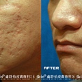
蔡依倫醫師

蔡依倫醫師與周慧敏合影

秋冬美白

new02

NEW01

蔡依倫醫師與郭雪芙廣告07

蔡依倫醫師專科化妝水01

蔡依倫醫師專科化妝水02

蔡依倫醫師與郭雪芙03

蔡依倫醫師與郭雪芙04

蔡依倫醫師與郭雪芙05

蔡依倫醫師與郭雪芙06

蔡依倫醫師與郭雪芙廣告06

2013-04-17_114004

郭雪芙

部落格宣傳圖片

2013100478890433

2013100478911569

2013100479032545

_DSC0943

_DSC0945

_DSC0969

_DSC0956

_DSC0970

_DSC0971

_DSC0972

_DSC0973

980407356_o

980412504_o

987573571_o

980415112_o

980402546_o

980417875_o

MN06_001

2014-01-27_114534

2014-01-27_114545

2014-01-27_114451

2014-01-27_114503

2014-01-27_114521

2014-01-27_120349

冷凍減脂介紹

母親節

酷爾塑平冷卻減脂&玻尿酸&肉毒桿菌合一張

MEDCURAS保養品組

母親節

0402部落格banner

蔡佳芬醫師峇里島研習

六月新娘主視覺

我要參加六月新娘活動

輕脂電波-3

2014夏日活動

NEW官網-BANNER

0717私房話老實說-12

盧院長與于美人合照

0717私房話老實說

0717私房話老實說-1

0717私房話老實說-2

受訪男性調查

1000x300

1000x300

20141107

@@@@

20100703-B-01
aas

Image 6

zczc-1

卓義峰

未命名-1

20141117

iSkin年終慶活動開跑

iSkin年終慶活動開跑

1

2

3
2-01
上一頁下一頁
分享:


相片最新留言
此相簿內的相片目前沒有留言
此相簿內的相片出現在:
相簿列表資訊
- 最新上傳:
- 2018/08/31
- 全站分類:
- 時尚美妝
- 本日人氣:
- 0
- 累積人氣:
- 841

常見的半導體材料有矽、鍺、砷化鎵等
/
晶片測試
晶片處理高度有序化的本質增加了對不同處理步驟之間度量方法的需求。晶片測試度量裝置被用於檢驗晶片仍然完好且沒有被前面的處理步驟損壞。如果If the number of dies—the 積體電路s that will eventually become chips—當一塊晶片測量失敗次數超過一個預先設定的閾值時,晶片將被廢棄而非繼續後續的處理製程。
/
晶片測試
晶片處理高度有序化的本質增加了對不同處理步驟之間度量方法的需求。晶片測試度量裝置被用於檢驗晶片仍然完好且沒有被前面的處理步驟損壞。如果If the number of dies—the 積體電路s that will eventually become chips—當一塊晶片測量失敗次數超過一個預先設定的閾值時,晶片將被廢棄而非繼續後續的處理製程。
/
步驟列表
晶片處理
濕洗
平版照相術
光刻Litho
離子移植IMP
蝕刻(干法蝕刻、濕法蝕刻、電漿蝕刻)
熱處理
快速熱退火Annel
熔爐退火
熱氧化
化學氣相沉積 (CVD)
物理氣相沉積 (PVD)
分子束磊晶 (MBE)
電化學沉積 (ECD),見電鍍
化學機械平坦化 (CMP)
IC Assembly and Testing 封裝測試
Wafer Testing 晶片測試
Visual Inspection外觀檢測
Wafer Probing電性測試
FrontEnd 封裝前段
Wafer BackGrinding 晶背研磨
Wafer Mount晶圓附膜
Wafer Sawing晶圓切割
Die attachment上片覆晶
Wire bonding焊線
BackEnd 封裝後段
Molding模壓
Post Mold Cure後固化
De-Junk 去節
Plating 電鍍
Marking 列印
Trimform 成形
Lead Scan 檢腳
Final Test 終測
Electrical Test電性測試
Visual Inspection光學測試
Baking 烘烤
/
有害材料標誌
許多有毒材料在製造過程中被使用。這些包括:
有毒元素摻雜物比如砷、硼、銻和磷
有毒化合物比如砷化三氫、磷化氫和矽烷
易反應液體、例如過氧化氫、發煙硝酸、硫酸以及氫氟酸
工人直接暴露在這些有毒物質下是致命的。通常IC製造業高度自動化能幫助降低暴露於這一類物品的風險。
/
Device yield
Device yield or die yield is the number of working chips or dies on a wafer, given in percentage since the number of chips on a wafer (Die per wafer, DPW) can vary depending on the chips' size and the wafer's diameter. Yield degradation is a reduction in yield, which historically was mainly caused by dust particles, however since the 1990s, yield degradation is mainly caused by process variation, the process itself and by the tools used in chip manufacturing, although dust still remains a problem in many older fabs. Dust particles have an increasing effect on yield as feature sizes are shrunk with newer processes. Automation and the use of mini environments inside of production equipment, FOUPs and SMIFs have enabled a reduction in defects caused by dust particles. Device yield must be kept high to reduce the selling price of the working chips since working chips have to pay for those chips that failed, and to reduce the cost of wafer processing. Yield can also be affected by the design and operation of the fab.
Tight control over contaminants and the production process are necessary to increase yield. Contaminants may be chemical contaminants or be dust particles. "Killer defects" are those caused by dust particles that cause complete failure of the device (such as a transistor). There are also harmless defects. A particle needs to be 1/5 the size of a feature to cause a killer defect. So if a feature is 100 nm across, a particle only needs to be 20 nm across to cause a killer defect. Electrostatic electricity can also affect yield adversely. Chemical contaminants or impurities include heavy metals such as Iron, Copper, Nickel, Zinc, Chromium, Gold, Mercury and Silver, alkali metals such as Sodium, Potassium and Lithium, and elements such as Aluminum, Magnesium, Calcium, Chlorine, Sulfur, Carbon, and Fluorine. It is important for those elements to not remain in contact with the silicon, as they could reduce yield. Chemical mixtures may be used to remove those elements from the silicon; different mixtures are effective against different elements.
Several models are used to estimate yield. Those are Murphy's model, Poisson's model, the binomial model, Moore's model and Seeds' model. There is no universal model; a model has to be chosen based on actual yield distribution (the location of defective chips) For example, Murphy's model assumes that yield loss occurs more at the edges of the wafer (non-working chips are concentrated on the edges of the wafer), Poisson's model assumes that defective dies are spread relatively evenly across the wafer, and Seeds's model assumes that defective dies are clustered together.[25]
Smaller dies cost less to produce (since more fit on a wafer, and wafers are processed and priced as a whole), and can help achieve higher yields since smaller dies have a lower chance of having a defect. However, smaller dies require smaller features to achieve the same functions of larger dies or surpass them, and smaller features require reduced process variation and increased purity (reduced contamination) to maintain high yields. Metrology tools are used to inspect the wafers during the production process and predict yield, so wafers predicted to have too many defects may be scrapped to save on processing costs.[26]